Himax Technologies
History and Development
Himax (HIMX) Taiwan, its predecessor, was incorporated on June 12, 2001 as a limited liability company under the laws of the ROC. On April 26, 2005, the company established Himax Technologies Limited, an exempted company with limited liability under the Cayman Islands Companies Law, as a holding company to hold the shares of Himax Taiwan in connection with its reorganization and share exchange. On October 14, 2005, Himax Taiwan became its wholly owned subsidiary through a share exchange consummated pursuant to the ROC Business Mergers and Acquisitions Law through which the company acquired all of the issued and outstanding shares of Himax Taiwan, and the company issued ordinary shares to the shareholders of Himax Taiwan. Shareholders of Himax Taiwan received one of its ordinary shares in exchange for one Himax Taiwan common share. The share exchange was unanimously approved by shareholders of Himax Taiwan on June 10, 2005 with no dissenting shareholders and by the ROC Investment Commission on August 30, 2005 for its inbound investment in Taiwan, and on September 7, 2005 for its outbound investment outside of Taiwan. The company effected this reorganization and share exchange to comply with ROC laws, which prohibit a Taiwan incorporated company not otherwise publicly listed in Taiwan from listing its shares on an overseas stock exchange. The company's reorganization enables it to maintain its operations through its Taiwan subsidiary, Himax Taiwan, while allowing it to list its shares overseas through its holding company structure.1
On September 26, 2005, the company changed its name to “Himax Technologies, Inc.,” and on October 17, 2005, Himax Taiwan changed its name to “Himax Technologies Limited” upon the approval of shareholders of both companies and amendments to the respective constitutive documents. The company effected the name exchange in order to maintain continuity of operations and marketing under the trade name “Himax Technologies, Inc.,” which had been previously used by Himax Taiwan.
The company's ADSs have been listed on the NASDAQ Global Select Market since March 31, 2006. The company's ordinary shares are not listed or publicly traded on any trading markets.
In February 2007, the company completed the acquisition of Wisepal, currently known as Himax Semiconductor, Inc., a fabless semiconductor company focusing on the development of LTPS TFT-LCD drivers for small and medium-sized applications. This transaction strengthened its competitive position in the small and medium-sized product areas and further diversified its technology and product offerings. From time to time, Himax Technologies has also made minority investments in various companies for strategic purposes in the ordinary course of business.
In March 2007, the company established Himax Imaging, Inc., or Himax Imaging, which develops and markets CMOS image sensors with an initial focus on camera applications used in cell phones and notebook computers.
In July 2012, its subsidiary, Himax Display, completed the acquisition of Spatial Photonics, currently known as Himax Display (USA) Inc., a Delaware corporation engaged in the business of manufacturing and production of MEMS products.
The company's principal executive offices are located at No. 26, Zih Lian Road, Sinshih District, Tainan City 74148, Taiwan, Republic of China. The company's telephone number at this address is +886-6-505-0880. The company's registered office in the Cayman Islands is located at Cricket Square, Hutchins Drive, P.O. Box 2681, Grand Cayman KY1-1111, Cayman Islands. The company's telephone number at this address is +1-345-945-3901. In addition, Himax Technologies has offices in Hsinchu and Taipei, Taiwan; Foshan, Fuqing, Ningbo, Beijing, Shanghai, Shenzhen, Suzhou, Wuhan, Hefei, Qingdao, Chongqing, Xi’an and Xiamen, China; Tokyo, Japan; Asan-si and Bundang-gu, South Korea; and Irvine and Campbell, California, Minneapolis, Minnesota, USA.
Business Overview
Himax Technologies is a fabless semiconductor solution provider dedicated to display imaging processing technologies. Himax Technologies is a worldwide market leader in display driver ICs and timing controllers used in TVs, laptops, monitors, mobile phones, tablets, digital cameras, car navigation, virtual reality (VR) devices and many other consumer electronics devices. Additionally, the company design and provide controllers for touch sensor displays, in-cell Touch and Display Driver Integration (TDDI) single-chip solutions, LED driver ICs, power management ICs, scaler products for monitors and projectors, tailor-made video processing IC solutions, silicon IPs and LCOS micro-displays for augmented reality (AR) devices and head-up displays (HUD) for automotive. The company also offer digital camera solutions, including CMOS image sensors and wafer level optics for AR devices, 3D sensing and machine vision, which are used in a wide variety of applications such as mobile phone, tablet, laptop, TV, PC camera, automobile, security, medical devices and Internet of Things. For display drivers and display-related products, its customers are panel manufacturers, agents or distributors, module manufacturers and assembly houses. The company also work with camera module manufacturers, optical engine manufacturers, and television system manufacturers for various non-driver products. The company believe that its recognized leading design and engineering expertise, combined with its focus on customer service and close relationships with semiconductor manufacturing service providers, has contributed to its success.
Industry Background
The company mainly operate in the flat panel display semiconductor industry. As the majority of its revenues derive from products that are critical components of flat panel displays, such as display drivers, timing controllers, scalers, power ICs and other semiconductor products, its industry is closely linked to the trends and developments of the flat panel display industry.
Flat Panel Display Semiconductors
Flat panel displays require different semiconductors depending upon the display technologies and the applications. Some of the most important ones include the following:
- Display Driver. The display driver receives image data from the timing controller and delivers precise analog voltages or currents to create images on the display. The two main types of display drivers for a TFT-LCD panel are gate drivers and source drivers. Gate drivers turn on the transistor within each pixel cell on the horizontal line on the panel for data input at each row. Source drivers receive image data from the timing controller and generate voltage that is applied to the liquid crystal within each pixel cell on the vertical line on the panel for data input at each column. The combination determines the colors generated by each pixel. Typically multiple gate drivers and source drivers are installed separately on the panel. However, for certain small and medium-sized applications, gate drivers and source drivers are integrated into a single chip due to space and cost considerations. Large-sized panels typically have higher resolution and require more display drivers than small and medium-sized panels.
- Timing Controller. The timing controller receives image data and converts the format for the source drivers’ input. The timing controller also generates controlling signals for gate and source drivers. Typically, the timing controller is a discrete semiconductor in large-sized TFT-LCD panels. For certain small and medium-sized applications, however, the timing controller may be integrated with display drivers.
- Scaler. For certain displays, a scaler is installed to magnify or shrink image data in order for the image to fill the panel.
- Operational Amplifier. An operational amplifier supplies the reference voltage to source drivers in order to make their output voltage uniform.
- Television Chipset. Television flat panel displays require chipsets that typically contain all or some of the following components: an audio processor, analog interfaces, digital interfaces, a video processor, a channel receiver and a digital television decoder. See “—Products—TFT-LCD Television and Monitor Semiconductor Solutions—TFT-LCD Monitor Chipsets” for a description of these components.
- Power IC. Power ICs include certain drivers, amplifiers, DC to DC converters and other semiconductors designed to enhance power management, such as voltage regulation, voltage boosting and battery management.
- Touch controller IC. For touch screen applications, touch controller ICs enable touch interfaces, such as capacitive touch panels, to identify, qualify and track user’s contacts with precision and sensibility.
- Others. Flat panel displays also require multiple general purpose semiconductors such as memory, power converters and inverters.
Characteristics of the Display Driver Market
Although the company operate in several distinct segments of the flat panel display semiconductor industry, its principal products are display drivers. Display drivers are critical components of flat panel displays. The display driver market has specific characteristics, including those discussed below.
Concentration of Panel Manufacturers
The global TFT-LCD panel industry consists of a small number of manufacturers, substantially all of which are based in Asia. In recent years, TFT-LCD panel manufacturers, in particular Taiwan- , Korea- and China-based manufacturers, have invested or are planning to invest heavily to establish, construct and ramp up additional fab capacity. The capital intensive nature of the industry often results in TFT-LCD panel manufacturers operating at a high level of capacity utilization in order to reduce unit costs. This tends to create a temporary oversupply of panels, which reduces the average selling price of panels and puts pricing pressure on component companies including display driver companies. Moreover, the concentration of panel manufacturers permits major panel manufacturers to exert pricing pressure on display driver companies such as it. The small number of panel manufacturers exacerbates this situation as display driver companies, in addition to seeking to expand their customer base, must also focus on winning a larger percentage of such customers’ display driver requirements.
Customization Requirements
Each panel display has a unique pixel design to meet its particular requirements. To optimize the panel’s performance, display drivers have to be customized for each panel design. The most common customization requirement is for the display driver company to optimize the gamma curve of each display driver for each panel design. Display driver companies must work closely with their customers to develop semiconductors that meet their customers’ specific needs in order to optimize the performance of their products.
Mixed-Signal Design and High-Voltage CMOS Process Technology
Display drivers have specific design and manufacturing requirements that are not standard in the semiconductor industry. Some display drivers require mixed-signal design since they combine both analog and digital devices on a single semiconductor to process both analog signals and digital data. Manufacturing display drivers require high-voltage CMOS process technology operating typically at 4.5 to 24 volts for source drivers and 10 to 50 volts for gate drivers, levels of voltage which are not standard in the semiconductor industry. For display drivers, the driving voltage must be maintained under a very high degree of uniformity, which can be difficult to achieve using standard CMOS process technology. However, manufacturing display drivers does not require very small-geometry semiconductor processes. Typically, the manufacturing process for large panel display drivers require geometries between 0.11 micron and 1 micron because the physical dimensions of a high-voltage device do not allow for the economical reduction in geometries below this range. The company believe that there are a limited number of fabs with high-voltage CMOS process technology that are capable of high-volume manufacturing of display drivers.
Special Assembly and Testing Requirements
Manufacturing display drivers requires certain assembly and testing technologies and equipment that are not standard for other semiconductors and are offered by a limited number of providers. The assembly of display drivers typically uses either tape-automated bonding, also known as TAB, or chip-on-glass, also known as COG, technologies. Display drivers also require gold bumping, which is a process in which gold bumps are plated onto each wafer to connect the die and the processed tape, in the case of TAB packages, and the glass, in the case of COG packages. TAB may utilize tape carrier packages, also known as TCP, or chip on film, also known as COF. The type of assembly used depends on the panel manufacturer’s design, which is influenced by panel size and application and is typically determined by the panel manufacturers. Display drivers for large-sized applications typically require TAB package types and, to a lesser extent, COG package types, whereas display drivers for mobile handsets and consumer electronics products typically require COG packages. The testing of display drivers also requires special testers that can support high-channel and high-voltage output semiconductors. Such testers are not standard in the semiconductor industry.
Supply Chain Management
The manufacturing of display drivers is a complex process and requires several manufacturing stages such as wafer fabrication, gold bumping, and assembly and testing, and the availability of materials such as the processed tape used in TAB packaging. The company refer to these manufacturing stages and material requirements collectively as the “supply chain.” Panel manufacturers typically operate at high levels of capacity utilization and require a reliable supply of display drivers. A shortage of display drivers, or a disruption to this supply, may disrupt panel manufacturers’ operations since replacement supplies may not be available on a timely basis or at all, given the customization of display drivers. As a result, a display driver company’s ability to deliver its products on a timely basis at the quality and quantity required is critical to satisfying its existing customers and winning new ones. Such supply chain management is particularly crucial to fabless display driver companies that do not have their own in-house manufacturing capacity. In the case of display drivers, supply chain management is further complicated by the high-voltage CMOS process technology and the special assembly and testing requirements that are not standard in the semiconductor industry. Access to this capacity also depends in part on display driver companies having received assurances of demand for their products since semiconductor manufacturing service providers require credible demand forecasts before allocating capacity among customers and investing to expand their capacity to support growth.
Need for Higher Level of Integration
The small form factor of mobile handsets and certain consumer electronics products restricts the space for components. Small and medium-sized panel applications typically require one or more source drivers, one or more gate drivers and one timing controller, which can be installed as separate semiconductors or as an integrated single-chip driver. Customers are increasingly demanding higher levels of integration in order to manufacture more compact panels, simplify the module assembly process and reduce unit costs. Display driver companies must be able to offer highly integrated chips that combine the source driver, gate driver and timing controller, as well as semiconductors such as memory, power circuit and image processors, into a single chip. Due to the size restrictions and stringent power consumption constraints of such display drivers, single-chip drivers are complex to design. For large-sized panel applications, integration is both more difficult to achieve and less important since size and weight are less of a priority. Lastly, as its TFT-LCD panel customers had turned to pure in-cell TDDI panel development for thinner display designs, Himax Technologies has developed a series of single chip touch display driver integrated circuit (TDDI) for advanced in-cell touch display panel.
Products and Solutions
Himax Technologies has several principal product lines:
- display drivers and timing controllers;
- touch controller ICs;
- TFT-LCD television and monitor semiconductor solutions;
- IP and ASIC service;
- LCOS and MEMS products;
- power ICs;
- CMOS image sensor products;
- wafer level optics products; and
- 3D sensing total solutions.
Display Drivers and Timing Controllers
Display Driver Characteristics
Display drivers deliver precise analog voltages and currents that activate the pixels on panels. The following is a summary of certain display driver characteristics and their relationship to panel performance.
- Resolution and Number of Channels. Resolution refers to the number of pixels per line multiplied by the number of lines, which determines the level of fine detail within an image displayed on a panel. For example, a color display screen with 1,024 x 768 pixels has 1,024 red columns, 1,024 green columns and 1,024 blue columns for a total of 3,072 columns and 768 rows. The red, green and blue columns are commonly referred to as “RGB.” Therefore, the display drivers need to drive 3,072 column outputs and 768 row outputs. The number of display drivers required for each panel depends on the resolution of the panel and the number of channels per display driver. For example, an XGA (1,024 x 768 pixels) panel requires eight 384-channel source drivers (1,024 x 3 = 384 x 8) and three 256-channel gate drivers (768 = 256 x 3), while a full HD (1,920 x 1,080 pixels) panel requires eight 720-channel source drivers and four 270-channel gate drivers. The number of display drivers required can be reduced by using drivers with a higher number of channels. For example, a full HD panel can have six 960-channel source drivers instead of eight 720-channel source drivers. Thus, using display drivers with a higher number of channels can reduce the number of display drivers required for each panel, although display drivers with a higher number of channels typically have higher unit costs.
- Color Depth. Color depth is the number of colors that can be displayed on a screen, which is determined by the number of shades of a color, also known as gray scale, that can be shown by the panel. For example, a 6-bit source driver is capable of generating 26 x 26 x 26 = 218, or 262K colors, and similarly, an 8-bit source driver is capable of generating 16 million colors. Typically, for TFT-LCD panels currently in commercial production, 262K, 16 million and 1 billion colors are supported by 6-bit, 8-bit and 10-bit source drivers, respectively.
- Operational Voltage. A display driver operates with two voltages: the input voltage (which enables it to receive signals from the timing controller) and the output voltage (which, in the case of source drivers, is applied to liquid crystals and, in the case of gate drivers, is used to switch on the TFT device). Source drivers typically operate at input voltages from 3.3 to 1.8 volts and output voltages ranging from 7 up to 18 volts. Gate drivers typically operate at input voltages from 3.3 to 1.8 volts and output voltages ranging from 10 to 50 volts. Lower input voltage saves power and lowers electromagnetic interference, or EMI. Output voltage may be higher or lower depending on the characteristics of the liquid crystal (or diode), in the case of source drivers, or TFT device, in the case of gate drivers.
- Gamma Curve. The relationship between the light passing through a pixel and the voltage applied to it by the source driver is nonlinear and is referred to as the “gamma curve” of the source driver. Different panel designs and manufacturing processes require source drivers with different gamma curves. Display drivers need to adjust the gamma curve to fit the pixel design. Due to the materials and processes used in manufacturing, panels may contain certain imperfections which can be corrected by the gamma curve of the source driver, a process which is generally known as “gamma correction.” For certain types of liquid crystal, the gamma curves for RGB cells are significantly different and thus need to be independently corrected. Some advanced display drivers feature three independent gamma curves for RGB cells.
- Driver Interface. Driver interface refers to the connection between the timing controller and display drivers. Display drivers increasingly require higher bandwidth interface technology to address the larger data volume necessary for video images. Panels used for higher data transmission applications, such as televisions, require more advanced interface technology. The principal types of interface technologies are transistor-to-transistor logic, or TTL, reduced swing differential signaling, or RSDS, mini-low voltage differential signaling, or mini-LVDS, and point-to-point high speed interface. Among these, RSDS, mini-LVDS and point-to-point interface were developed as low power, low noise and low amplitude methods for high-speed data transmission using fewer copper wires and resulting in lower EMI. Moreover, there are some panel manufacturers developing their proprietary point-to-point interfaces, such as embedded panel interface, or EPI, USI-T, iSP, CEDS, CHPL, CDPI and CMPI.
- Package Type. The assembly of display drivers typically uses TAB and COG package types. COF and TCP are two types of TAB packages, of which COF packages have become predominantly used in recent years. Customers typically determine the package type required according to their specific mechanical and electrical considerations. In general, display drivers for small-sized panels use COG package types, whereas display drivers for large-sized panels primarily use TAB package types and, to a lesser extent, COG package types.
Large-Sized Applications
The company provide source drivers, gate drivers, PMIC, P-gamma OP and timing controllers for large-sized panels principally used in desktop monitors, notebook computers and televisions. Display drivers used in large-sized applications feature different key characteristics, depending on the end-use application. For example, the industry trend for large-sized applications is generally toward super high channel, low power consumption, low cost, thin and light form factor, touch function, higher data transmission rate and higher driving capabilities. Higher speed interface technologies are also key for 4Kx2K and 8K high-resolution TVs. Greater color depth, enhanced color through RGB independent gamma and 3D display, are particularly important for advanced televisions and certain monitors.
In February 2009, the company introduced timing controllers with the content adaptive brightness control, or CABC, technology. CABC technology controls backlight brightness intelligently by analyzing the content displayed to save power and enhance the contrast level while maintaining vivid display quality. The company's algorithm enables a smooth adjustment in backlight brightness even when the content changes swiftly.
For notebook interface, its eDP 1.1 and eDP 1.2 timing controllers began mass production in 2011 and 2012 respectively. The company's eDP 1.3 timing controller entered mass production in 2013 and was also adopted in the world’s lightest notebook by its top-tier notebook brand customer. In 2015, the company launched ultra-low power consumption eDP 1.4 timing controller that pairs with Nvidia G-Sync and AMD FreeSync™ technologies for graphic cards to process 3D graphics on ultra-high resolution displays in tablets, notebooks and monitors applications. These technological innovations were successfully adopted by various tier-one system customers in the following year. In 2017, its eDP timing controller that supports 4K UHD notebook began mass production. Eyeing on the growing gaming hardware and HDR market, the company will advance its solutions to provide the best user experience in 2018.
In December 2010, Himax introduced programmable gamma OP with VCOM to provide reference voltages in TFT-LCD panels. Mass production of this product started in the second half of 2012. Programmable gamma OP is an individual component from driver IC and contains 8 to 16 programmable 10-bit DAC outputs and 1 to 2 voltage reference for VCOM. The VCOM reference voltage has its own 10-bit DAC and an amplifier to guarantee stable voltage when critical levels and patterns are displayed. Each DAC can be programmed separately by a 10-bit word to 1024 values.
Core Technologies and Know-How
Driving System Technology. Through its collaboration with panel manufacturers, Himax Technologies has developed extensive knowledge of circuit design, TFT-LCD driving systems, high-voltage processes and display systems, all of which are important to the design of high-performance TFT-LCD display drivers. The company's engineers have in-depth knowledge of the driving system technology, which is the architecture for the interaction between the source driver, gate driver, timing controller and power systems as well as other passive components. The company believe that its understanding of the entire driving system has strengthened its design capabilities. The company's engineers are highly skilled in designing power efficient and compact display drivers that enhance the performance of TFT-LCD. Himax Technologies is leveraging its know-how of display drivers and driving system technology to develop display drivers for panels utilizing other technologies such as OLED.
High-Voltage CMOS Circuit Design. Unlike most other semiconductors, TFT-LCD display drivers require a high output voltage of 3.3 to 50 volts. Himax Technologies has developed circuit design technologies using a high-voltage CMOS process that enables it to produce high-yield, reliable and compact drivers for high-volume applications. Moreover, its technologies enable it to keep the driving voltage at very high uniformity, which can be difficult to achieve when using standard CMOS process technology.
3D Technologies. Several technologies in Himax are integrated together to form its 3D solution. First, wafer level imprinted technology is used to design and manufacture DOE and WLO. Then, the totally new design CMOS sensor architecture and process gives the industry leading NIR Quantum Efficiency (QE) sensors which are specially designed for 3D applications. The company's expertise in precision assembly in optics as well as ASIC and driver design additionally helps it to provide a more complete solution to its customers.
High-Bandwidth Interfaces. In addition to high-voltage circuit design, TFT-LCD display drivers require high bandwidth transmission for video signals. Himax Technologies has applied several high-speed interfaces, including transistor-transistor logic (“TTL”), Reduced Swing Differential Signaling (“RSDS”), mini low-voltage differential signaling (“LVDS”), dual-edge TTL (“DETTL”), turbo Reduced Swing Differential Signaling (“RSDS”), Mobile Industry Processor Interface (“MIPI”)and other customized interfaces, in its display drivers. Moreover, Himax Technologies is developing additional driver interfaces for special applications with optimized speed, lower EMI and higher system stability.
Die Shrink and LowPower Technologies. The company's engineers are highly skilled in employing their knowledge of driving technology and high-voltage CMOS circuit design to shrink the die size of its display drivers while leveraging their understanding of driving technology and panel characteristics to design display drivers with low power consumption. Die size is an important consideration for applications with size constraints. Smaller die size also reduces the cost of the chip. Lower power consumption is important for many portable devices such as notebook computers, mobile handsets and consumer electronics products.
Customers
The company's customers for display drivers are primarily panel manufacturers and mobile device module manufacturers, who in turn design and market their products to manufacturers of end-use products such as notebook computers, desktop monitors, televisions, mobile handsets and consumer electronics products. The company may sell its products through agents or distributors for certain products or in certain regions. As of December 31, 2017, the company sold its products to more than 200 customers. The company's ten largest customers together accounted for approximately 74.3%, 76.4% and 75.3% of its revenues in 2015, 2016 and 2017, respectively. In 2015, 2016 and 2017, its two largest customers accounted for 10% or more of its net revenue: customer A and its affiliates, accounted for 20.1%, 22.4% and 25.8% of its revenues, respectively; customer B and its affiliates, accounted for 21.1%, 15.2% and 15.5% of its revenues, respectively.
Certain of its customers provide it with a long-term (twelve-month) forecast plus three-month rolling non-binding forecasts and confirm orders about one month ahead of scheduled delivery. In general, purchase orders are not cancellable by either party, although from time to time the company and its customers have agreed to amend the terms of such orders.
Sales and Marketing
The company focus its sales and marketing strategy on establishing business and technology relationships principally with TFT-LCD panel manufacturers, panel manufacturers using LTPS or OLED, or Oxide technologies, mobile display module and mobile device manufacturers and camera module houses in order to work closely with them on future semiconductor solutions that align with their product road maps. The company's engineers collaborate with its customers’ engineers to create products that comply with their specifications and provide a high level of performance at competitive prices and also create customized features for end brand customers. The company's end market for large-sized panels is concentrated among a limited number of major panel manufacturers. The company also market its products directly to monitor, notebook and mobile device manufacturers so that its products can be qualified for their specifications and designed into their products. Furthermore, the company extend its business development with system and ODM companies by using strategic ASIC business model to not only develop ASIC product based on customer specification but also jointly research and develop new technologies to meet customers' future product demand. Additionally, the company will form a strategic partnership with tier-1 customers for its LCOS microdisplays to penetrate into an emerging market. The company believe the company need this close relationship with its customers to create a new application eco system.
The company primarily sell its products through its direct sales teams located in Taiwan, China, South Korea and Japan. The company also have dedicated sales teams for certain of its most important current or prospective customers. Himax Technologies has offices in Tainan, Hsinchu, Taipei, Taiwan; and Shenzen and Suzhou, China. Himax Technologies has other sales and technical support offices in Hefei, Beijing, Shanghai, Fuzhou, Foshan, Fuqing, Ningbo, Wuhan, Qindao, Chongqing, Xi’an and Xiamen, China; Tokyo, Japan; Asan-si and Bundang-gu, South Korea; and Irvine and Campbell, California, USA, all in close proximity to its customers. For certain products or regions, the company may sell its products through agents or distributors.
The company's sales and marketing team possesses a high level of technical expertise and industry knowledge used to support a lengthy and complex sales process. This includes a highly trained team of product managers and field applications engineers. The company's team is equipped with extensive strategic marketing experience and a strong capability to identify market trends. The company also provide technical support and assistance to potential and existing customers in system/SoC architecture, designing, testing and qualifying display modules, camera modules and end application systems that incorporate its products and ASICs. The company believe that the depth and quality of this design support are key to improving customers’ time-to-market and maintaining a high level of customer satisfaction.
Manufacturing
The company operate primarily in a fabless business model that utilizes substantially third-party foundry and assembly and testing capabilities. The company leverage its experience and engineering expertise to design high-performance semiconductors and rely on semiconductor manufacturing service providers for wafer fabrication, gold bumping, assembly and testing. The company also rely largely on third-party suppliers of processed tape used in TAB packaging. The company engage foundries with high-voltage CMOS process technology for its display drivers and engage assembly and testing houses that specialize in TAB and COG packages, thereby taking advantage of the economies of scale and the specialization of such semiconductor manufacturing service providers. The company's primarily fabless model enables it to capture certain financial and operational benefits, including reduced manufacturing personnel, capital expenditures, fixed assets and fixed costs. It also gives it the flexibility to use the technology and service providers that are the most suitable for any given product.
The company operate a fab under Himax Display primarily for performing manufacturing processes for its LCOS microdisplays. Moreover, for better integration, the company also established an in-house color filter facility under Himax Taiwan, which commenced shipments from 2010. This in-house facility provides color filter for CMOS image sensor products with over 50 million optics shipment record to tier-1 customers and LCOS products. The color filter line is a critical and unique process for its proprietary single-panel color LCOS microdisplays. An in-house color filter facility enhances the competitiveness of its LCOS products and creates value for its customers. In addition, Himax Technologies has established an in-house WLO facility under Himax Taiwan for the key process of its wafer level optics products, which commenced small-scale shipments in December 2009.
Manufacturing Stages
The diagram below sets forth the various stages in manufacturing display drivers according to the two different types of assembly utilized: TAB or COG. The assembly type depends primarily on the application and design of the panel and is determined by its customers.
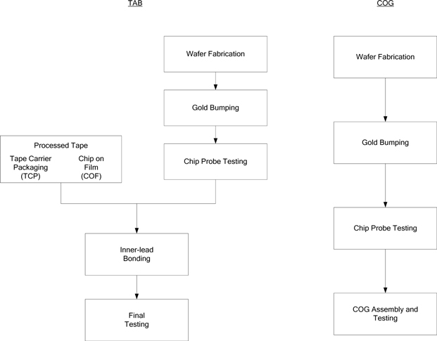
Wafer Fabrication: Based on its design, the foundry provides it with fabricated wafers. Each fabricated wafer contains many chips, each known as a die.
Gold Bumping: After the wafers are fabricated, they are delivered to gold bumping houses where gold bumps are plated on each wafer. The gold bumping process uses thin film metal deposition, photolithography and electrical plating technologies. The gold bumps are plated onto each wafer to connect the die to the processed tape, in the case of TAB package, or the glass, in the case of COG package.
Chip Probe Testing: Each die is electrically tested, or probed, for defects. Dies that fail this test are discarded.
Assembly and Testing: The company's display drivers use two types of assembly technology: TAB or COG. Display drivers for large-sized applications typically require TAB package types and to a lesser extent COG package types, whereas display drivers for mobile handsets and consumer electronics products typically require COG package types.
TAB Assembly
The company use two types of TAB technologies: TCP and COF. TCP and COF packages are both made of processed tape that is typically 35mm or 48mm wide, plated with copper foil and has a circuit formed within it. TCP and COF packages differ, however, in terms of their chip connections. With TCP packages, a hole is punched through the processed tape in the area of the chip, which is connected to a flying lead made of copper. By contrast, with COF packages, the lead is mounted directly on the processed tape and there is no flying lead. In recent years, COF packages have become predominantly used in TAB technology.
- Inner-Lead Bonding: The TCP and COF assembly process involves grinding the bumped wafers into their required thickness and cutting the wafers into individual dies, or chips. An inner lead bonder machine connects the chip to the printed circuit processed tape and the package is sealed with resin at high temperatures.
- Final Testing: The assembled display drivers are tested to ensure that they meet performance specifications. Testing takes place on specialized equipment using software customized for each product.
COG Assembly
COG assembly connects display drivers directly to LCD panels without the need for processed tape. COG assembly involves grinding the tested wafers into their required thickness and cutting the wafers into individual dies, or chips. Each individual die is picked and placed into a chip tray and is then visually or auto-inspected for defects. The dies are packed within a tray in an aluminum bag after completion of the inspection process.
Quality Assurance
The company maintain a comprehensive quality assurance system. Using a variety of methods, from conducting rigorous simulations during the circuit design process to evaluating supplier performance at various stages of its products’ manufacturing process, the company seek to bring about improvements and achieve customer satisfaction. In addition to monitoring customer satisfaction through regular reviews, the company implement extensive supplier quality controls so that the products the company outsource achieve its high standards. Prior to engaging a third party as its supplier, the company perform a series of audits on their operations, and upon engagement, the company hold frequent quality assurance meetings with its suppliers to evaluate such factors as product quality, production costs, technological sophistication and timely delivery.
In November 2002, the company received ISO 9001 certification, which was renewed in February 2017 and will expire in September 2018. In February 2006, the company received ISO 14001 certification, which was renewed in December 2017 and will expire in December 2020. In addition, in March 2007, the company received IECQ QC 080000 certification, which was renewed in March 2016 and will expire in March 2019, and OHSAS 18001 certification, which was renewed in December 2017 and will expire in January 2021.
Semiconductor Manufacturing Service Providers and Suppliers
Through its relationships with leading foundries, assembly, gold bumping and testing houses and processed tape suppliers, the company believe Himax Technologies has established a supply chain that enables it to deliver high-quality products to its customers in a timely manner.
Access to semiconductor manufacturing service providers is critical as display drivers require high-voltage CMOS process technology and specialized assembly and testing services, all of which are different from industry standards. Himax Technologies has obtained its foundry services from TSMC, Vanguard, Macronix, Globalfoundries Singapore, SMIC and Maxchip in the past few years and have also established relationships with UMC, HHNEC, PSC and SK Hynix. These are among a select number of semiconductor manufacturers that provide high-voltage CMOS process technology required for manufacturing display drivers. The company engage assembly and testing houses that specialize in TAB and COG packages such as Chipbond, Chipmore International trading company Ltd., ChipMOS Technologies Inc., Nepes Corporation and King Yuan Electronics Co., Ltd.
The company plan to strengthen its relationships with its existing semiconductor manufacturing service providers and diversify its network of such service providers in order to ensure access to sufficient cost-competitive and high-quality manufacturing capacity. Himax Technologies is selective in its choice of semiconductor manufacturing service providers. It takes a substantial amount of time to qualify alternative foundries, gold bumping, assembly and testing houses for production. As a result, the company expect that the company will continue to rely on a limited number of semiconductor manufacturing service providers for a substantial portion of its manufacturing requirements in the near future.
The table below sets forth (in alphabetical order) its principal semiconductor manufacturing service providers and suppliers:
| Wafer Fabrication | Gold Bumping |
|---|---|
| Globalfoundries Singapore Pte., Ltd. | Chipbond Technology Corporation |
| Macronix International Co., Ltd. | Chipmore International Trading Company Ltd. |
| Maxchip Electronics Corp. | ChipMOS Technologies Inc. |
| Powerchip Technology Corporation | LB Semicon Co., Ltd. |
| Semiconductor Manufacturing International Corporation | Nepes Corporation |
| Shanghai Hua Hong NEC Electronics Company, Ltd. | Union Semi Conductor Co., Ltd. |
| SK Hynix | |
| Taiwan Semiconductor Manufacturing Company Limited | |
| United Microelectronics Corporation | |
| Vanguard International Semiconductor Corporation | |
| Processed Tape for TAB Packaging | Assembly and Testing |
| JMC Electronics Co., Ltd. | Ardentec Corporation |
| LG Innotek Co., Ltd. | Advanced Semiconductor Engineering Inc. |
| Stemco., Ltd. | Chipbond Technology Corporation |
| Chipmore International Trading Company Ltd. | |
| ChipMOS Technologies Inc. | |
| Global Testing Corporation | |
| Greatek Electronics Inc. | |
| Jiangsu Changjiang Electronics Technology Co., Ltd. | |
| King Yuan Electronics Co., Ltd. | |
| Micro Silicon Electronics Corp. | |
| Nepes Corporation | |
| Orient Semiconductor Electronics Ltd. | |
| Taiwan IC Packaging Corporation | |
| Chip Probe Testing | |
| Ardentec Corporation | |
| Chipbond Technology Corporation | |
| Chipmore International Trading Company Ltd. | |
| ChipMOS Technologies Inc. | |
| Global Testing Corporation | |
| Greatek Electronics Inc. | |
| King Yuan Electronics Co., Ltd. | |
| Micro Silicon Electronics Corp. | |
| Nepes Corporation | . |
Intellectual Property
As of February 28, 2018, the company held a total of 2,990 patents, including 1,356 in Taiwan, 939 in the United States, 619 in China, and 76 in other countries. The expiration dates of its patents range from 2019 to 2038. The company also have a total of 93 pending patent applications in Taiwan, 113 in the United States and 227 in other jurisdictions, including the PRC, Japan, Korea and Europe. In addition, Himax Technologies has registered “Himax” and its logo as a trademark and service mark in Taiwan, China, Europe, Singapore, Korea and Japan and the United States.
Organizational Structure
The following chart sets forth its corporate structure and ownership interest in each of its principal operating subsidiaries and affiliates as of February 28, 2018.
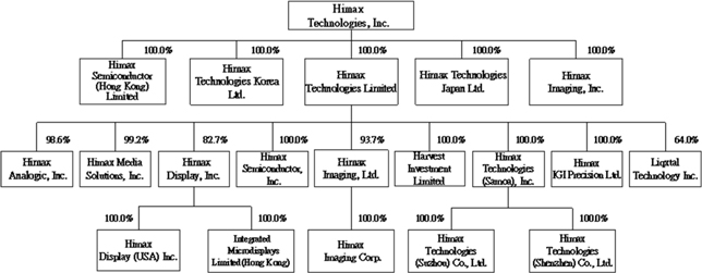
The following table sets forth summary information for its subsidiaries as of February 28, 2018.
| Subsidiary | Main Activities | Jurisdiction of Incorporation | Percentage of Our Ownership Interest |
|---|---|---|---|
| Himax Technologies Limited | IC design and sales | ROC | 100 |
| Himax Technologies Korea Ltd. | IC design and sales | South Korea | 100 |
| Himax Semiconductor, Inc. | IC design and sales | ROC | 100 |
| Himax Technologies (Samoa), Inc. | Investments | Samoa | 100 |
| Himax Technologies (Suzhou) Co., Ltd. | Sales and technical support | PRC | 100 |
| Himax Technologies (Shenzhen) Co., Ltd. | Sales and technical support | PRC | 100 |
| Himax Display, Inc. | LCOS and MEMS design, manufacturing and sales | ROC | 82.7 |
| Integrated Microdisplays Limited | LCOS design | Hong Kong | 82.7 |
| Himax Display (USA) Inc. | LCOS and MEMS design, sales and technical support | Delaware, USA | 82.7 |
| Himax Analogic, Inc. | IC design and sales | ROC | 98.6 |
| Himax Imaging, Inc. | Investments | Cayman Islands | 100 |
| Himax Imaging, Ltd. | IC design and sales | ROC | 93.7 |
| Himax Imaging Corp. | IC design | California, USA | 93.7 |
| Himax Media Solutions, Inc. | TFT-LCD television and monitor chipset operations, ASIC service and IP Licensing | ROC | 99.2 |
| Harvest Investment Limited | Investments | ROC | 100 |
| Himax Technologies Japan Ltd. | Sales | Japan | 100 |
| Himax Semiconductor (Hong Kong) Limited | Investments | Hong Kong | 100 |
| Liqxtal Technology Inc. | LC Lens design and sales | ROC | 64 |
| Himax IGI Precision Ltd. | 3D micro and nano structure mastering and prototype replication | Delaware, USA | 100 |


